PECVD: Revolutionizing Thin Film Deposition

Semiconductors are becoming an essential part of technological advancement. People use semiconductors in electronics, communications, computing, healthcare, military systems, and transportation. Plasma enhanced chemical vapor deposition (PECVD) is one way to manufacture semiconductors.
The PECVD method offers the semiconductor industry a reliable and reproducible process but that’s not all, it can also be used to create solar cells, optics, and coatings.
Advantages of PECVD
PECVD is a technique that uses plasma to deposit thin films of materials on a substrate, or underlying, surface. It differs from conventional chemical vapor deposition (CVD) because it deposits films at lower temperatures, typically ranging between 200- 400°C. This method protects temperature-sensitive materials by eliminating the need to heat the chamber or substrate.
“This is achieved through the generation of free ions necessary for the deposition process without resorting to high thermal energy. Instead, PECVD utilizes electric and/or magnetic fields to excite the desired atoms or molecules, creating the necessary ions for deposition,” EMA PhD Senior Scientist Gregory Wilson said.
PECVD also allows for more rapid deposition. For example, silicon nitride deposition rates are 160 times faster during PECVD compared to CVD. Further, the PECVD process is able to create films with different properties by adjusting the plasma parameters and gas composition. PECVD also produces films of high quality and uniform thickness ensuring good adhesion while reducing the risk of cracking. On top of that, the PECVD method is ideal for working with complex surfaces containing intricate shapes or structures. Films have also demonstrated very high solvent and corrosion resistance with chemical and thermal stability.
The Working Mechanism of PECVD
PECVD takes place in a vacuum chamber equipped with gas inlets, a pressure gauge, and temperature controller. A stand holds the substrate inside the chamber that can control temperature and potential. Figure 1 is a simple illustration of a PECVD chamber.

Simple illustration of a PECVD chamber.
PECVD systems generate deposition species by applying a cyclical electric or magnetic field within the chamber using electrodes. The electrodes are separate but parallel with one connected to an RF power supply and the other grounded. This forces the substrate to create a bias potential. It works similarly to a capacitor in an electric circuit.
The PECVD process typically starts with the introduction of precursor gases into the chamber housing the substrate, these can include silane (SiH4) and ammonia (NH3). They are mixed with inert gases like argon or nitrogen to control processes.
“The excited electrons, mobilized by these fields, collide with neutral species injected into the chamber at controlled flow rates, leading to ionization,” Wilson said. “As ionization progresses, a plasma of excited electrons and ions is formed and diffuses throughout the chamber.”
An electrical discharge of 100- 300 eV between the electrodes is used to create the plasma. The ions, energized by their interaction with the electric fields, efficiently bind to the substrate’s surface, allowing for precise buildup of thin films.
When the process is finished, the system pumps away any chemical bi-products.
PECVD is generally performed in pressures <0.1 Torr. This allows for low substrate temperatures and uniformity in the deposition process. This method can deposit a variety of films, such as silicon oxide (SiO2), silicon nitrate (Si3N4), silicon carbide (SiC), diamond-like carbon, and amorphous silicon.
Changing Results
Properties can be changed to get different results. For instance, a higher gas flow rate correlates to a higher deposition rate. By varying the parameters of the plasma, users can control qualities such as thickness, hardness, or refractive index. Different parameters that can be controlled include:
- RF frequency
- Flow rate of the neutral species
- Geometry of the electrodes
- Distance between the substrate and the electrodes
- Inlet configuration
- External circuitry connected to the system
“Each of these factors can significantly alter both plasma generation and the subsequent deposition processes, highlighting the importance of meticulous system calibration,” Wilson said.
Applications and Industry Impact
PECVD finds extensive application in the processing of silicon and similar materials thanks to its non-damaging deposition capabilities. It plays a pivotal role in various industries but particularly in nanotechnology, solar cell production, and electronics.
“In the fabrication of solar cells, PECVD is instrumental in depositing the thin films required for efficient energy conservation,” Wilson said. “Similarly, in the electronics sector, it ensures the creation of high-quality, reliable components essential for modern devices.”
The nanoscale PECVD market is seeing significant growth, with a market forecast value of $5.1B in 2031. Growth factors include:
- Increasing demand for miniaturized devices
- Rising investments along with research and development
- Surge in renewable energy solutions
- Advancement in semiconductor technology
Current trends are shaping the trajectory of the industry. Manufacturers are working to incorporate eco-friendly practices by using environmentally friendly precursor gases. Researchers are using artificial intelligence (AI) to optimize PECVD parameters, enhance efficiency, and reduce production costs. Companies are partnering together to leverage strengths, share resources, and accelerate innovation.
Advancing PECVD
To further enhance the precision and efficiency of the PECVD processes, EMA has developed a sophisticated simulation tool designed to fine-tune the countless complex parameters involved.
Our product Ansys Charge Plus is capable of advanced plasma and gas flow modeling to simulate the diverse aspects of PECVD. It combines:
- A Finite Element Method (FEM) solver for electric and magnetic fields
- A Particle-in-Cell (PIC) solver for kinetic particle motion
- A fluid solver for bulk species movement
- A reaction solver for both gas and surface reactions
- Complex sheath models to manage kinetic effects within the sheath
- A circuit solver to handle intricate circuitry connected to the electrodes, substrate, and other boundaries
“By employing advanced time stepping management, complex meshing considerations, and other necessary methodologies, EMA’s tool enables accurate and robust analysis of PECVD systems,” Wilson said. “This capability not only improves the efficiency of the PECVD process but also extends to other plasma-based processes such as etching, providing valuable insights and optimizations.”
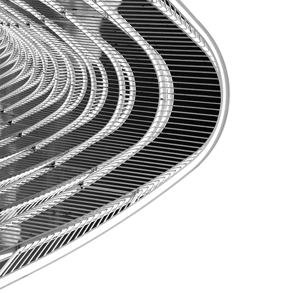
PECVD Chamber
Figure 2 is a look inside of a PECVD chamber model showing the electron density. Charge Plus allows users to look at the density enhancements in the system, temperature distributions, and the flow of the fluid inside the chamber based on settings set at start of the simulation.
Adaptive mesh group layers in Charge Plus support the PECVD workflow. Instead of requiring the same size mesh throughout the model, users can add a very small mesh to solve for very thin regions of plasmas that could be present near the electrodes. This feature also allows users to examine plasma sheaths, which are critical for the calculation of electromagnetic fields and the distribution of particles inside the chamber.
Figure 3 illustrates the adaptive mesh in an argon plasma chamber with the sheath shown in very fine detail. This example demonstrates how the acceleration scheme enables very small RF cycles and how the plasma responds to the RF electromagnetic field on small scales while maintaining its stability on longer time scales.
STart now
PECVD stands out as transformative technology in thin film deposition. It provides significant advantages over traditional methods by preserving material integrity through low-temperature processes. The applications across nanotechnology, solar cells, and electronics underscore its vital role in advancing current and future technological innovations. With EMA’s cutting-edge simulation tool, the precision and efficiency of PECVD processes are further elevated, paving the way for continued advancements in the field.
Ansys is the exclusive seller of Charge Plus, you can learn more by clicking here.
If you’re ready to get simulating with EMA, click here.